Annotated Lab Report Template
The following is a template to clarify what should be part of the writeup you post for each lab you complete. It is a sample report written to explain a simple FPGA blink demo. Each section contains a brief explanation of the purpose of the section and the information that should be included in it.
Introduction
Briefly explain what was done.
In this lab, a design was implemented on the FPGA to demonstrate the functionality of the on-board high-speed oscillator by blinking one of the on-board LEDs. The high speed oscillator was configured at a frequency of 24 MHz and divided down using a counter to achieve a blinking frequency of ~1.5 Hz.
Design and Testing Methodology
Explain how you approached the design of this assignment from both a software and a hardware standpoint (as appropriate). Include how you tested your design. These tests should convince the reader that the requirements of the assignment have been met.
The on-board high-speed oscillator (HSOSC) from the iCE40 UltraPlus primitive library was used to generate a clock signal at 24 MHz. Then, a counter was used to divide the high frequency clock signal down so that the blinking frequency could be easily visualized using one of the on-board LEDs.
The design was developed using a simple clock divider module which drives the external LED.
Technical Documentation:
Include a link to a Git repository with your Verilog code, a block diagram of your design, and schematics of your circuits.
The source code for the project can be found in the associated Github repository.
Block Diagram
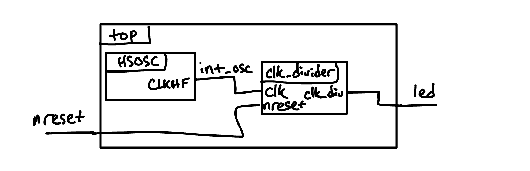
The block diagram in Figure 1 demonstrates the overall architecture of the design. The top-level module top includes two submodules: the high-speed oscillator block (HSOSC) and the clock divider module (clk_divider). Every net and port in the block diagram must be labeled – that means each wire at the top level has to have a name, and the connection to a submodule must show the name inside the module. This is true even if the submodule port name is the same as the top level net name.
Schematic
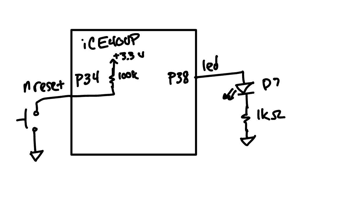
Figure 2 shows the physical layout of the design. An internal 100 k\(\Omega\) pullup resistor was used to ensure the active low reset pin was not floating. The output LED was connected using a 1 k\(\Omega\) current-limiting resistor to ensure the output current (~2.6 mA) did not exceed the maximum output current of the FPGA I/O pins.
Results and Discussion
Did you accomplish all of the prescribed tasks? If not, what are the shortcomings? How might you address them given more time? As appropriate, how did the design perform (e.g., How fast/accurate/reliable was it?).
Testbench Simulation
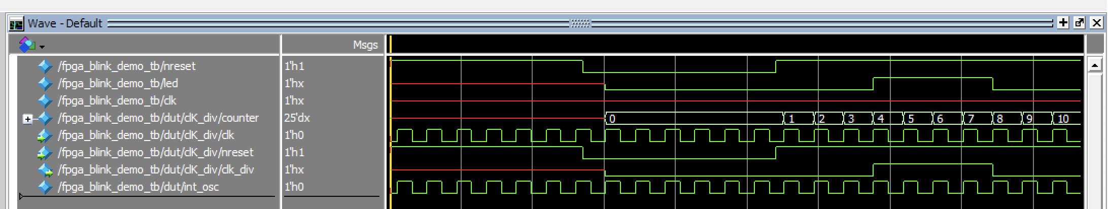
The design met all intended design objectives. Figure 3 shows a screenshot of the QuestaSim simulation. If a more precise output frequency was desired, a more sophisticated counter could be developed. The current design only allows for the clock to be divided by powers of two.
Conclusion
Briefly summarize what was done and how it performed. Also note how many hours you spent working on the lab.
The design successfully blinked an external LED using the on-board high-speed oscillator. I spent a total of two hours working on this lab.
AI Prototype Summary
Include generated code, easy-to-read chat transcripts, and a reflection on how well it worked.