Hardware Background
Background
In the 1980’s and 1990’s, digital design projects were built from a truckload of chips, each containing a few logic gates such as 74xx series logic gates or simple programmable array logic chips (PALs). Such projects involve placing and wiring together dozens of chips on a breadboard. It was easy to make a wiring mistake or burn out a chip and spend hours tracking down the problem. Now you can perform all of your digital logic on a single field-programmable gate array (FPGA) to greatly reduce the necessary wiring and number of chips. Later in the course, you will use the Cortex-M4 microcontroller to write programs in assembly language and C that can interface with external hardware and the FPGA.
Nucleo-L432KC Development Board
The Nucleo-L432KC development board provides a convenient platform to test and develop embedded systems applications. The board is focused around an STM32L432KC MCU and provides voltage regulators to provide power to the chip, various breakout headers which allow access to the pins of the microcontroller chip, a reset button and user input button, configuration jumpers, and an embedded ST-LINK programmer/debugger.
Programming
The STM32L432KC has an embedded ST-LINK/V2-1 programmer and debugger as described in the Nucleo-32 User Manual. The main purpose of the ST-LINK is to provide the ability to interface with the serial wire debug (SWD) interface of the MCU via USB.
There are a variety of integrated development environments (IDEs) which can be used to interact with the device including PlatformIO, Keil μVision, and SEGGER Embedded Studio. The IDEs provide a helpful wrapper around compiler toolchains such as GNU Compiler Collection (GCC) toolchain to facilitate easy programming and debugging. In this course you are welcome to use any IDE you would like, although instruction and support will be focused around SEGGER Embedded Studio which is based on the GCC toolchain.[^1]
UPduino v3.1 FPGA Development Board
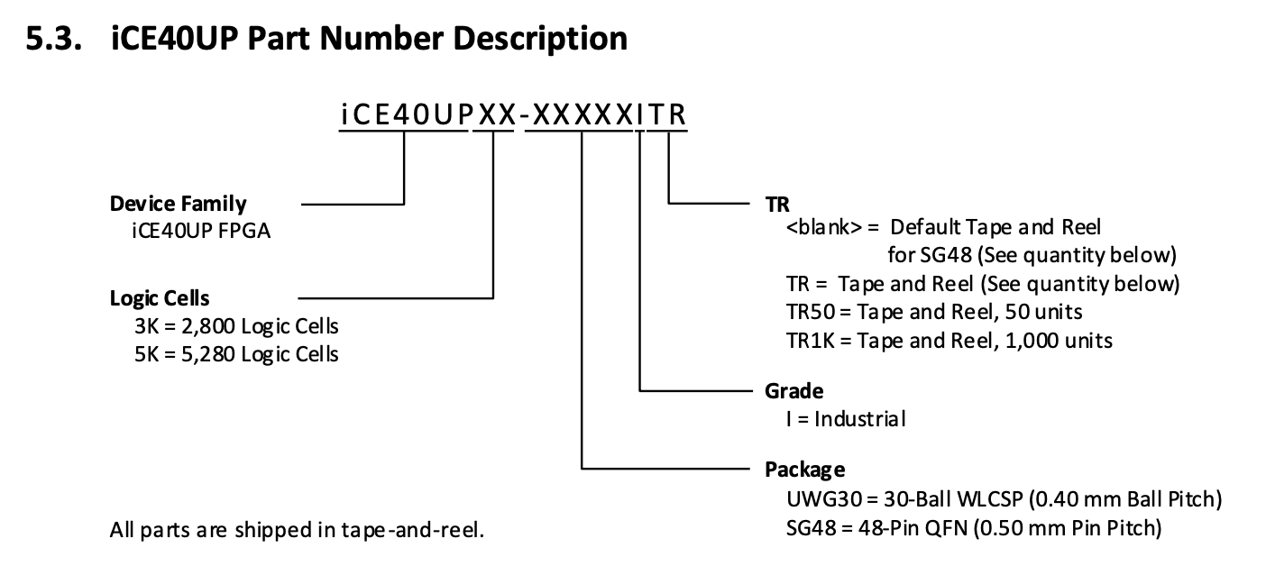
The UPduino v3.1 is developed by tinyvision.ai and designed around a Lattice Semiconductor UP5K field programmable gate array (FPGA). Section 5.3 of the iCE40 UltraPlus Family Data Sheet (FPGA-DS-02008-2.0) explains the naming of the chip.
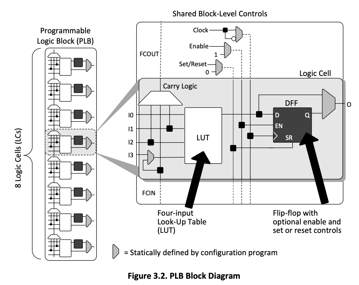
The Lattice UP5K is very similar to the Cyclone IV architecture that is used to introduce FPGAs in E85. At its root, the FPGA consists of Logic Cells (Lattice’s version of the Intel/Altera Logic Elements you learned about in E85) which can be internally connected within Programmable Logic Blocks (PLBs) within the FPGA to form digital circuits. Each Logic Cell (LC) consists of a 4-input look-up table (LUT) and a programmable D flip-flop, along with additional clock control and carry logic. Figure 3.2 from the FPGA datasheet shows the basic architecture of a PLB and LC.
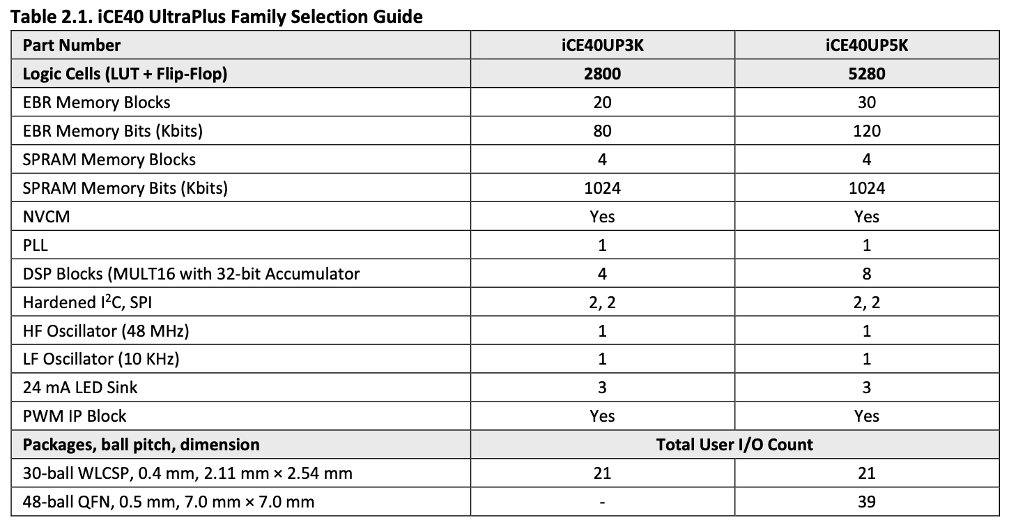
The UP5K on our UPduino v3.1 board is the 48-pin QFN package. As you can see from the table, it contains 5280 logic cells, 30 Embedded Block Ram (EBR) Memory Blocks of 4 Kbits each, 4 256-bit Single Port synchronous RAM Memory Blocks, and an on-board high-frequency (48 MHz) and low-frequency (10 kHz) oscillator.
Digital Design Synthesis and Programming
The FPGA is programmed using the onboard programmer via the synthesis tool Lattice Radiant. After setting up and compiling the Radiant project, Radiant will generate bitstream files which are used to configure the FPGA.
More details will be provided later in this lab writeup.