E155 Development Board
Board Overview
In this lab you will assemble a custom printed circuit board which hosts the MCU and FPGA boards. The board has several features that will be convenient for developing embedded systems such as:
- Pins which can be directly routed from the MCU to the FPGA via the board
- Extension headers for the mikroBUS and 6-pin PMOD standard
- User configurable LEDs, pushbuttons, and slider switches.
- Header to route pins via a ribbon cable to a separate breadboard adapter PCB which can be inserted into a solderless breadboard.
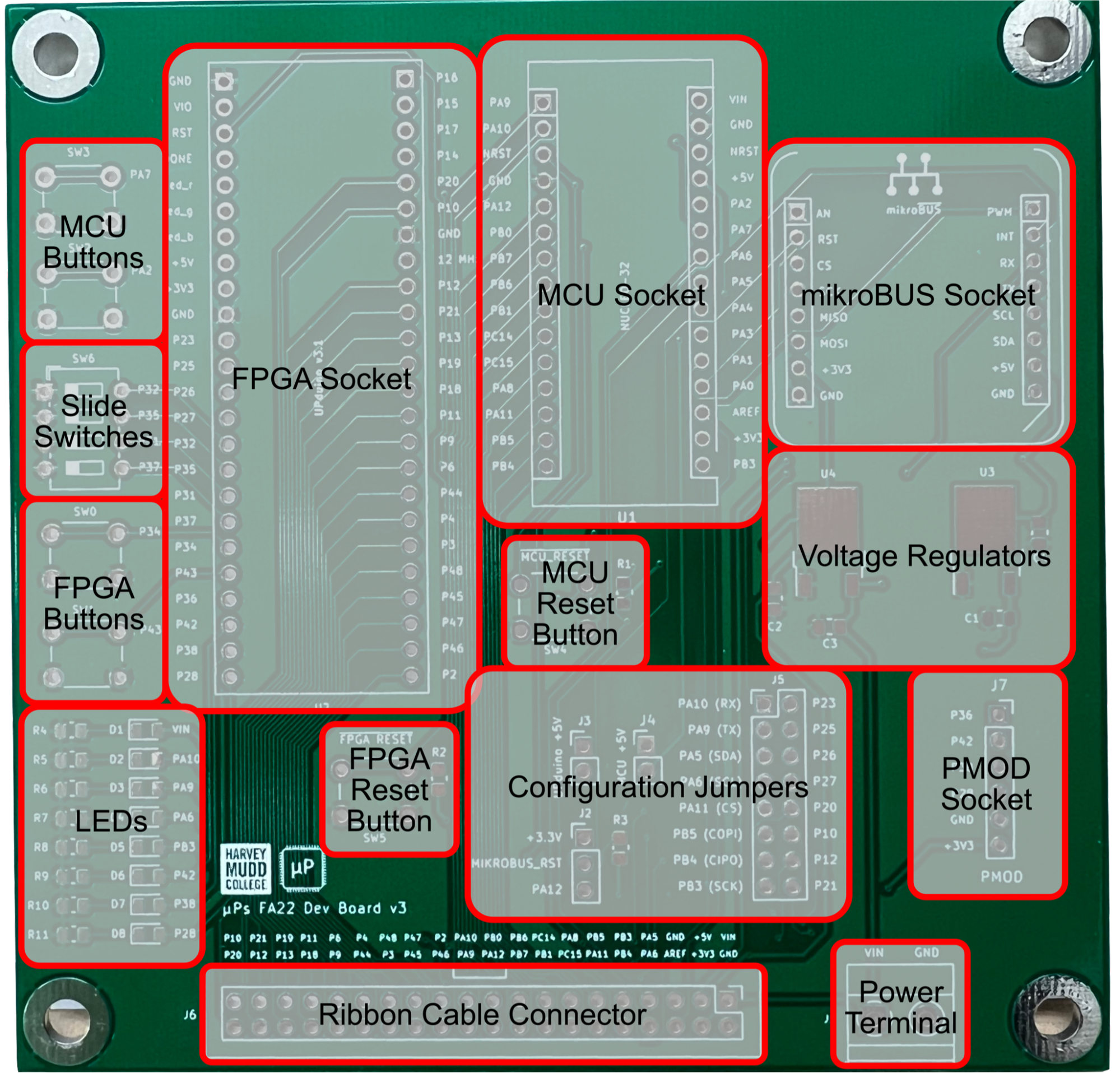
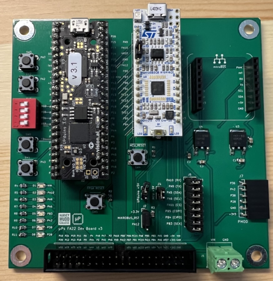
The board has several main sections that you should make yourself aware of. They are annotated in the image above.
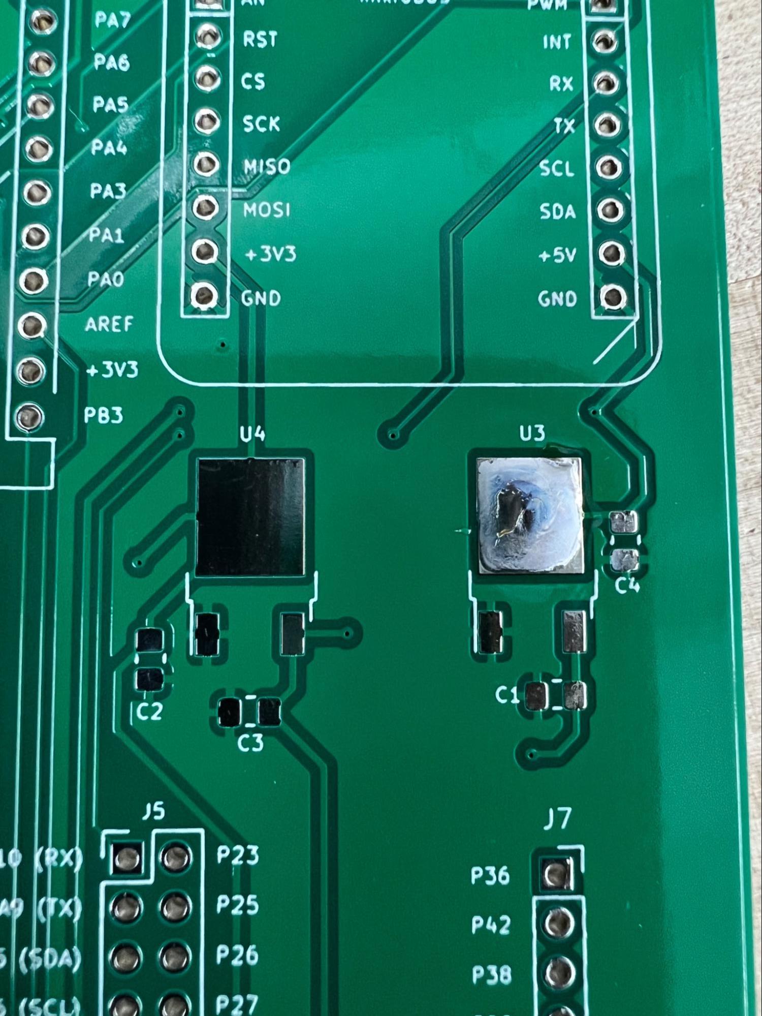
- Voltage Regulators and Power Terminal: A +5 V (NCP1117DT50RKG) and +3.3 V (NCP1117DT33T5G) low-dropout (LDO) voltage regulator which is used to regulate the input provided via the power terminal on VIN. Make sure to check with the schematic to ensure that you put the regulators in their proper places. See Powering the Board for more details.
- FPGA, MCU, mikroBUS, and PMOD sockets: These sockets are populated with female headers for the MCU, FPGA, and other extension sockets to be plugged into.
- Reset Push Buttons: The reset pushbuttons are connected to the reset inputs on the MCU and FPGA respectively. The MCU reset button will cause the code to begin execution from the first instruction. The FPGA reset button causes the FPGA to reconfigure itself from the on-board RAM which stores the configuration file for the design you have uploaded.
- Configuration Jumpers: The configuration jumpers on the board allow you several options to set the power and signal connections for the MCU and FPGA. J2, J3, and J4 control the mikroBUS reset signal and the power for the FPGA and MCU boards respectively. The mikroBUS reset signal can also be connected to MCU pin PA12 to enable the MCU to reset the connected peripheral via software. The configuration jumper J5 is a 2x8 header with MCU pins on the left hand side and FPGA pins on the right hand side. Note that on version v4 of the board, J5 has been replaced with an 8-pin DIP switch with the reference designator SW7. The functionality however, remains the same as the jumper. By attaching a jumper between the pins in the same row, the MCU pin on the left side of the jumper can be directly routed to the FPGA pin on the right hand side via traces on the PCB. This allows for convenient and high-fidelity interfaces between the MCU and the FPGA without the need for external wires.
- Ribbon Cable Connector: The ribbon cable connector is used to route a subset of the MCU and FPGA pins out to a cable which connects to the breadboard adapter board.
- MCU, FPGA, and Slide Buttons: The push and slide buttons on the board are routed to pins on the MCU and FPGA in order to provide on-board options to toggle GPIO pins on the respective devices. Note that all of these buttons are configured as active low (i.e., closing the switch connects the pin of the device to ground) without any hardware pullup resistors. In order to use them, you must configure the internal pullup resistors on the MCU or FPGA in order to avoid floating logic levels.
Assembling the Board
In this section you will walk through the steps to assemble your board. The PCB has both through hole technology (THT) and surface mount technology (SMT) parts. SMT parts are generally preferred on PCBs since they are more compact and easier for machines to solder although THT parts are typically easier for beginners to solder. If you haven’t done much (or any!) SMT soldering before, don’t worry! One of the points of this lab is to give you a chance to develop this skill!
All the parts you need to build your board are provided in your kit bag. Typically, it is easiest to start with the SMT parts before soldering the THT parts since the board will lay flat. So we’ll start by soldering the SMT components.
Assembly Tips
Soldering is a skill that you need to practice just like anything else. The most important thing to remember when soldering is that it is roughly 100x easier to solder than to desolder a component. So, whenever possible, make sure that you align the component correctly before soldering all the pins. Often the best way to do this is to solder a single pin on one side and then confirm that the component is correctly aligned before soldering the rest of the pins. If something is misaligned, then this will make it easy to correct since you only will need to reflow a single solder joint. A few additional tips:
- Soldering often will make you wish you had another hand or two. Soldering SMT components in particular can be a bit tricky because you need to hold the component with tweezers to align it. A good strategy is to first melt a little bit of solder on one of the pads and then grab the component with tweezers while holding the iron in your other hand to reflow the solder and align it.
- When soldering THT headers like those used for the sockets, make sure that the headers are oriented correctly (most of the time perpendicular to the PCB surface). One tip is to insert a strip of male headers into a breadboard and then attach the female headers and set the PCB upside down on top of the male headers to solder them. If you do end up making a mistake and need to desolder a strip of header pins, the plastic shroud can be removed in order to let you pull out individual pins. See this YouTube video for an example. Although in the video he shows the example for a male header pin strip, you can do the same thing with a female strip as well.
Suggested Soldering Order
Below is a recommended soldering order.
- Solder the voltage regulators. Put a bit of solder on the big square pad and reflow while bringing the regulator on top in order to solder it. You can apply heat to the pad via the metal edge at the top of the regulator.
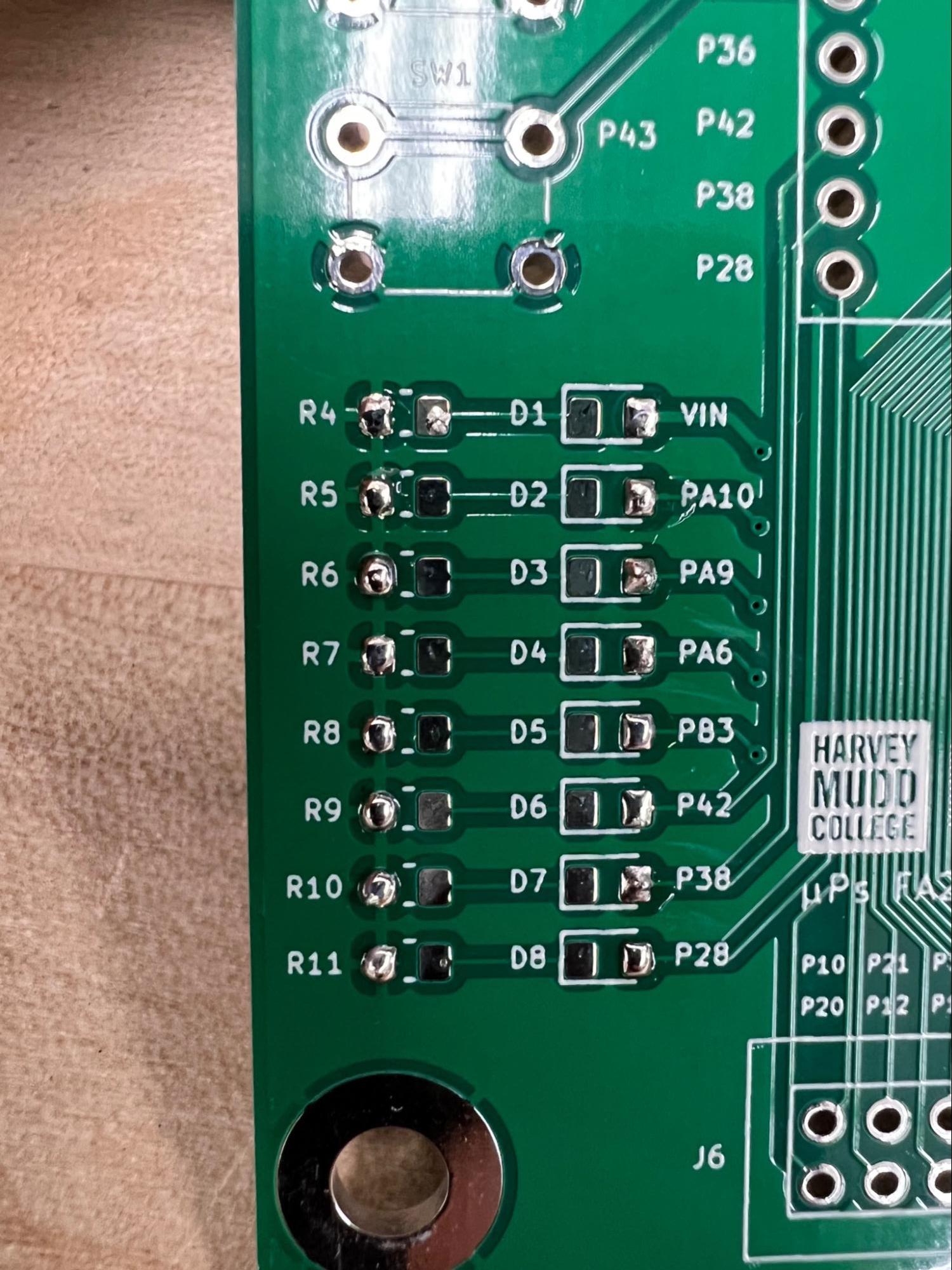
- Prepare to solder the remaining SMT components (resistors, capacitors, and LEDs) by applying a small amount of solder to one pad of the SMT footprints R1-R11, C1-C4, and D1-D8..
- Solder the decoupling (also known as bypass) capacitors C1-C4 around the regulators. These are used to smooth out any transients and ensure smooth, constant voltages. These capacitors have no polarity, so either way is fine.
- Next, solder the resistors on the board. Pay careful attention to make sure that you solder the correct resistors by referring to the board schematic (available on the course website).
- Next solder the LEDs. The LEDs are polarized, so you’ll need to make sure to solder them the right direction or they won’t work. There is an arrow on the bottom of the package which indicates the direction of the current flow from the anode to the cathode. Again, refer to the schematic for proper alignment. When looking at the PCB with the text facing upright, the cathode should go on the left hand side (connected to its current limiting resistor). There are three different color LEDs. D1 is red (VIN), D2-D5 are green (connected to the MCU), and D6-D8 are blue (connected to the FPGA). After finishing this step, you are finished with all the SMT components!
- Now it’s time to tackle the THT components. Put the components into their respective places and solder them in. Pay careful attention to ensure that the female header strips are correctly aligned and perpendicular to the board. You will need to snap off 2- and 3-pin headers from the provided 40-pin header strip in order to populate J2-J4. The easiest way to do this is to use a pair of needle nose pliers to snap off the right number of pins. Do not solder the UPduino or the Nucleo directly to your board. Populate U2 and U1 with female header sockets.
- After finishing the main development board, follow the same procedure to assemble the breadboard adapter PCB.
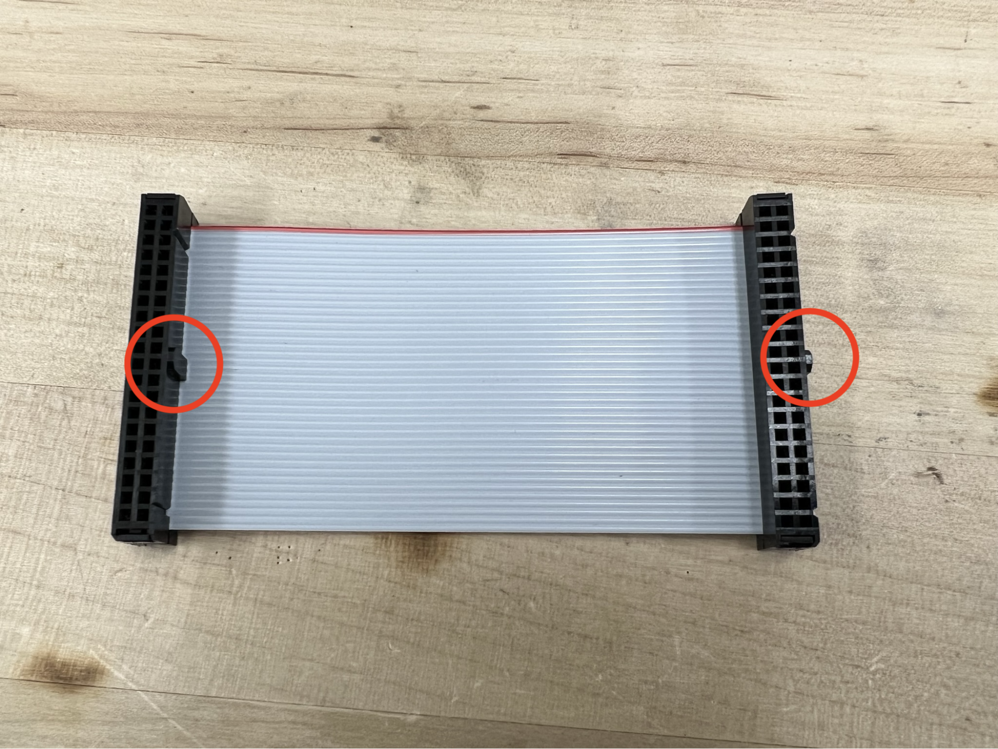

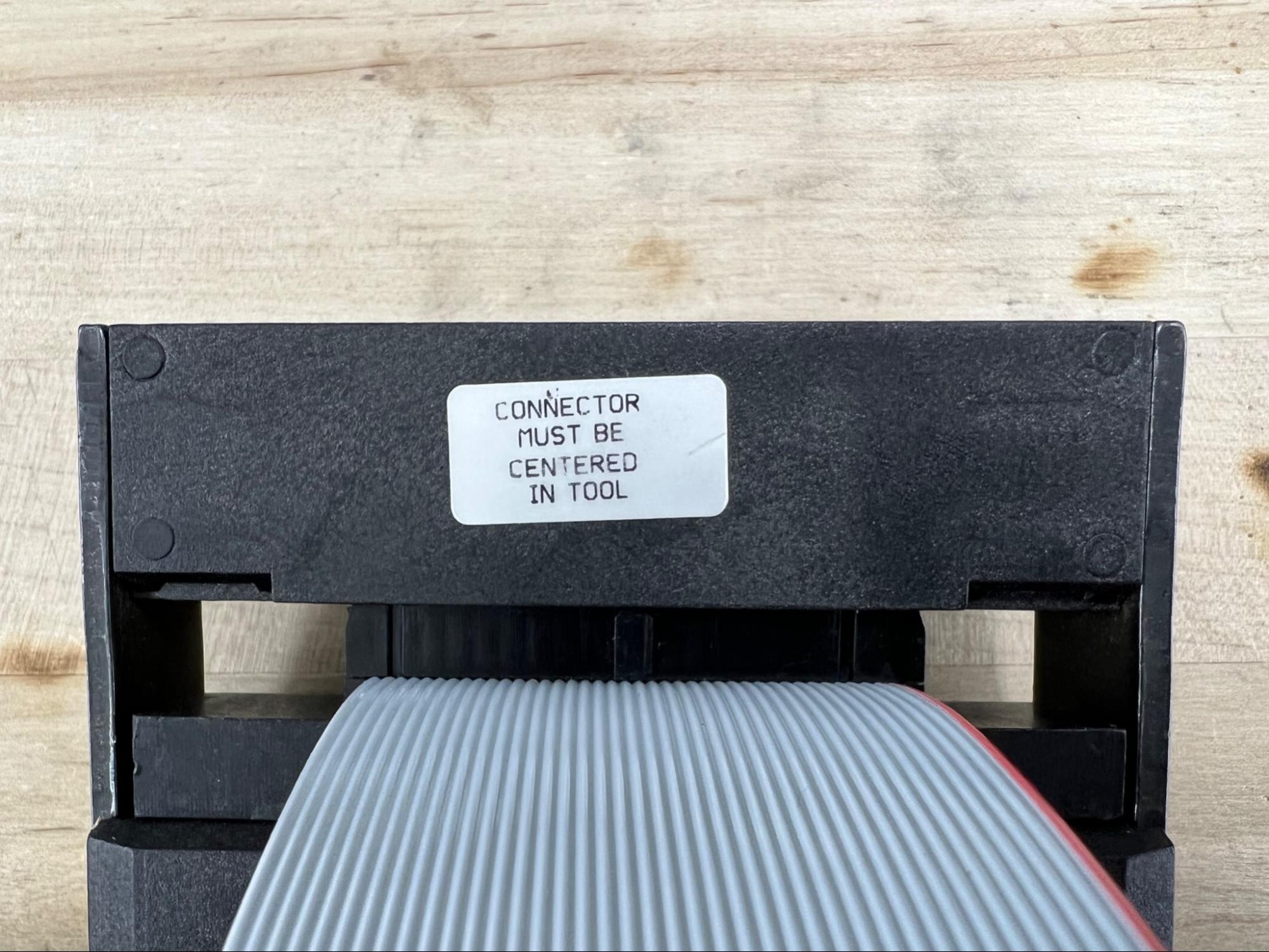
Use the included insulation-displacement contact (IDC) ribbon cable connectors and the spool of ribbon cable in the lab to make yourself a short (~6-12”) cable. You have probably done this before in E80, but if you don’t remember how, see the video here. Cut the cable to length with the flush cutters in the toolbox and use either a vise or the cable assembly tool found in the E155 cabinet. Please make sure to put it back after you are finished. If you can’t find it around the lab, ask an instructor.
Finally, solder the 20-pin male headers and 2x20 pin cable connector onto the breadboard adapter PCB, making sure that the pins are all correctly aligned and perpendicular to the PCB.
Congratulations, you are now finished assembling your board and ready to test it! The photo below shows an example of what the board should look like when it is finished.
Powering the Board
There are three different ways to power the components on the development board: (1) via the VIN power input, (2) via the FPGA’s USB connection, and (3) via the MCU’s USB connection. In this section we will walk through the various ways to power the board to make sure that you are aware of how to properly power the board and avoid any issues which might damage the components on board.
The +5 V and +3.3 V voltage regulators provide power for the various components. All logic levels are +3.3 V unless stated otherwise. So, the +3.3 V supply is used to power the various buttons on the board.
Powering through VIN
To power through VIN, apply a voltage to the power screw terminal between VIN and GND. The NCP117 series can accept voltages up to +20 V but in most scenarios you will likely want to use a VIN between +6-12 V. Be aware that VIN should always be more than +5 V for both regulators to function properly. When powering via VIN, the jumpers J3 (FPGA_+5V) and J4 (MCU_+5V) should be shorted in order to apply the +5 V output from the regulator to the MCU and FPGA +5 V pin.
Powering via USB
It is also possible to power the board via a USB connection to either the MCU or FPGA board. Each board has an onboard voltage regulator to create a stabilized +5 V output on the boards respective +5 V pins. Assuming J3 and J4 are shorted, this +5 V output from whichever board is connected to USB power is fed back to the +5 V line (which is also the output of the +5 V regulator) and thus powers the other components connected to that net.
Before connecting your MCU and FPGA boards, check the voltage regulators are on correctly by connecting to a lab DC power supply using the screw terminals and using a multimeter to confirm that the +3.3 V rail is +3.3 V and the +5 V rail is +5 V. If you read +5 V on the +3.3 V or vice versa, you have installed the regulators in the wrong place and need to swap them. If you read a low voltage (less than ~0.1 V), you likely have a bad solder joint on the back pad of the respective regulator and need to reflow the solder joint to make a better connection.
Testing the Boards
To test the boards, you will upload a simple design to the FPGA which toggles an LED on and off and some code on the MCU to read in the toggling GPIO pin and echo is back to the FPGA. This will ensure that the board is working properly and that you have good communication between the two devices.
To familiarize yourself with how to program the FPGA using Lattice Radiant, see the Lattice Radiant iCE40 UltraPlus Project Setup tutorial. This tutorial has information about how to create a project in Radiant and how to synthesize and upload designs to your FPGA board.
After working through the tutorial, download the Radiant project file fpga_dev_board_test.zip under the Lab 1 subfolder from the course GitHub and use it to program your FPGA. This design toggles pin P25 at about 1 Hz. If you have the switch properly set on SW7, P25 is connected to PA9 and so you will see LED D3 blinking.
After programming your FPGA, the next step is to upload the code to the MCU that will read the value of the toggled LED from the FPGA and echo it back on another pin. See the tutorial titled “Segger Embedded Studio Setup” to familiarize yourself with the process of installing and setting up SEGGER Embedded Studio (SES). If you are using a lab computer, SES is already installed. The lab computers may also have other versions installed.
After working through the tutorial, download the SES solution folder from the course GitHub titled mcu_dev_board_test.zip. Then, double click on the .emProject file or use the File → Open Solution option in SES to open the solution. This project contains a simple program that monitors the status of PA9 (which is connected to P25 through the appropriate jumper on J5. Make sure you have the jumper attached to connect PA9 to P25). Build and download the project to your MCU.
Now, in addition to LED D3 (PA9/P25) blinking, you should see LED D2 (PA10/P23) and LED D7 (P38) blinking as well.